domingo, 17 de abril de 2016

CFL Electronic Ballast 01

CFL stands for "Conmpact Fluorescent Lamp".
How do these new low energy consuming bulbs light-up? With electronic ballasts!
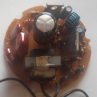
1. Description
I salvaged this electronic ballast from a CFL (before I knew there was mercury in the bulb...).
I didn't write down the power, but because of the size (board is 55 mm in diameter) it was a relatively large one, likely for 1000 lumen (220 V, E27 socket).

The board has the following marks:
BS-03
GH372

Two pictures:


2. Electronic Ballasts
"Electronic ballasts contain a small circuit board with a bridge rectifier, a filter capacitor and usually two switching transistors. The incoming AC current is first rectified to DC, then converted to high frequency AC by the transistors, connected as a resonant series DC to AC inverter. The resulting high frequency is applied to the lamp tube." (source

I have found the following documents regarding the history, functioning and design of electronic ballast of interest:
- Electronic Fluorescent Lamp Ballast, application note from STMicroelectronics,
- Electronic Lamp Ballast Design, also an application note from ON Semiconductor.

Unfortunately, my knowledge of electronics does not allow me (at least for now!) to be able to follow them.

There are some sites involved in tinkering/reverse-engineering these type of components:
- PAVOUK,
- SHADDAK
- Nuno Suceda.


3. Schematics and Components
I have tried to sketch the circuit in QUCS, as usual in this series, but I am not even able to clearly identify the components, so this will have to come later...

Toaster Controller A0201D

1. Description
I found few days ago a toaster on a street. I normally do not pick this type of gadgets because I feel that somebody else may use them for better - but this time I got the electronics.

Because I only got the control board, I do not know the model: it was a toaster for two-slices, with independent selectors and three operation buttons: "reheat", "cancel" and "defrost".

For each slice-heater there is a control, with two boards each: for the timer/controller and for the buttons. 

Pictures of the control board and buttons:


The boards are 80*50 mm and 105*20 mm.

They are connected by 5 cables, and they have the following marks:
KT-223-MAIN for the main board,
and
KT-223-KR or KT-223-KL for the button boards (right & left).

The main board has two additional connector sockets: one with two pins, which is for the relay activating the heating AC side, one with three pins, which is the DC power supply for the board.


2. ICs for Toasters
The IC at the core of this board is labelled as:
A0201D
TN1430G3C+

I have not managed to get the datasheet of the IC A0201D - this is probably related to an intelectual property issue, at least this is what I asume.

This youtube upload is titled A0201D, and clearly talks about a toaster (model Aurora AU 153). It also mentions IC PT8A2511. Unfortunately it's ... in Russian!

This other webpage has the European certificates and tests on a toaster. The certificate mentions two suppliers for the control board, and the use of A0201D for certain models from one manufacturer, and PT8A2511 for the same models made by the other manufacturer.

Here, somebody asks for the equivalent subtitute of the A021D IC on a Kenwood TTP112 toaster (no reply was provided). Here some German guys were fighting with another toaster using this same IC (in German!). And there are also some Hungarians having fun/troubles with the toaster and the IC, and quoting pages in Chinese!

(In this Babel Tower I'm only missing the Finns!)

The A0201D chip is not unheard of: it is possible to find it on sales pages (f.eg: here or here), but no way to find the datasheet...

At least, for what seems to be an alternative IC, the PT8A2511, a datasheet is readily available (see here). As per the Hungarian blog mentioned above: "The Russians dare to believe and 99.99% certainty that the IC is the same as the PT8A2511".

In this page, which may be a/the manufacturer of the A0201D, the supply voltage is mentioned to be 3.5-5.5 V (other sources mention 12 V for the control board of toasters).

So, all in all, I have managed to collect the following:

- The "EMC Emission Test Report" for an electric toaster in whose control board, for some models, is installed the A0201D IC, as well as the PT8A2511. (The document is skimmed of what is no relevant here). The following scheme is of special interest:


- The PT8A2511 IC datasheet. This is a "CMOS LSI chip designed for toaster", presented in DIP8 package and working at 3.5-4.5 V. It includes few more information besides this scheme:
- The GA5210PH IC datasheet. This is also a DIP8 IC for toasters. The document is mostly in Chinese, mentions a standard range of 9-12 V, and includes the following scheme (among others):

Despite the apparent differences, all schematics share the pin utilization of the IC:
PIN 1 : DEFROST
PIN 2 : REHEAT
PIN 3 : RELAY / OUTPUT
PIN 4 : VCC
PIN 5 : RX
PIN 6 : OSC / RC
PIN 7 : CX
PIN 8 : GND

As per the PT8A2511 datasheet, the PIN operation is as follows:


3. Schematics

The circuit is modeled in QUCS, and can be found here.
A snapshot of the schematics:

Remarks:
1. The IC A0201D is not a sub-circuit, it's only a "box" without functionality. On this regard the schematics is "useless".
2. The lights at the button board are not LEDs (or at least their resistance is equal in both directions...)
3. The power supply (6 V) is just a figure: as mentioned above, I'm not sure of the required voltage.
4. The switches at the button board are actually of the push-button type (momentary, they remain open unless they are kept pushed).


4. Operation
The board is powered from connections S3_3 (VCC) and S3_1 (GND).
The coil is powered through S2_2, but only activated if the transistor T1 is closed, whose base is controlled by  PIN3.
Pushing puttons DR1 or DR2 closes the circuit through ground to PIN1 (a negative pulse). Similarly, pushing puttons RR1 or RR2 closes the ciruit through ground to PIN2. These negative pulses, according to the previous table, activates the DEFROST or REHEAT timing, resp. Once the function is activated, PIN3 activates the AC relay.
Once PIN1 or PIN2 are activated, they generate a positive voltage which keeps on the lights in the button board (DEF and REH).
If the main board is powered, the POW light is on through the direct VCC-GND circuit, regardless of the position of CR1/CR2.
If CR1 or CR2 are closed, in addition, a branch is closed through the base of the transistor Q1. Whether the voltage at the base is enough to overcome the transistor resistance will depend on specific values, but if it can, then it will also activate the coil which controls the heating of the slices.
VCC to PIN4 is constant.
The variable resistors VR1&2 control voltage at PIN6, and then the frequency of the oscillating system and the duration of the pulses at PIN2 and PIN3.
PIN5 and PIN7 are likely starters for the time counter controlled by the oscillator.

domingo, 10 de abril de 2016

SCART board

1 Description
This is a SCART board from an old DVD player (if I'm not mistaken). The board size is 80*25 mm.

Some pictures:


The board has several marks:
LFM 200492-0001
76VCA
94V-0

Besides the female SCART connector it has two male pin sockets: one for 8 pins/cables, the other for 5.

2 Simulation
The circuit is modeled in QUCS, and can be found here.
A snapshot of the schematics:


There are a number of parts which seem to be ferrite beads: they are black cylinders, unmarked, the PCB labels them as FBNNN, and it makes sense that there are filters for signal cleaning. Their properties are unknown to me and I have simulated each of them as a subcircuit, with the model and properties mentioned here for one example. The impedances of all them is in the range of 0.5 ohm, as measured by my DMM.
There are also some SMD parts whose identification is unclear:
- ZDNNN, which I assume are Zener diodes protecting the line in case of voltage peaks (all are marked E29 except one (ZD135) which is H38).
- CNNN, which I asume are capacitors, but of unknown capacitance.

3 SCART
See here for information on the connections. The standard, EN 50049, is here.

There are several SCART connectors (at least three as per this source, in Spanish).

Pins 1, 2, 3 and 6 are for the audio (L and R, IN and OUT); the Zener protects lines 1 and 3 which are both OUT. This side goes to pin connector RB203.

All video signals are protected by Zener diodes, and go to pin connector RB202.

As per the pins used on the board, this is a type 1 connector. Pins (7, 11, 15) form the RGB channels IN, and pin 19 for composite video OUT; pins 8 and 16 control the communication acording to voltage levels (see here).
Voltage levels are (source here):
- Audio: 0.5 Vrms
- Video RGB: 0.7 Vrms
- pin 8:
* 0 - 2 V = no signal, or internal bypass
* 4.5 - 7 V (nominal 6 V) = widescreen (16:9) signal; (5-8 V as per this source).
* 9.5 - 12 V (nominal 12 V) = normal (4:3) signal
- pin 16:
* 0 - 0.4 V = composite
* 1 - 3 V (nominal 1 V) = RGB
- pin 19: 1 V   

All impedances from teh SCART female connector to the internal pin connectors are low (below 1 ohm as per my DMM).
 

sábado, 9 de abril de 2016

Power Source 01


1 Description
This is a small board (56+60 mm), whose origin I do not recall.

It seems a sort of noise filter: the main capacitors are as per EN132400, which seems to be a standard for capacitors in line filtering applications, so that the amount of radio/electromagnetic interferences generated by the equipment, and transmitted back to the supply line, is minimized. Two sources of information on this subjec: one and two.

Two pictures of the board:


It shows a mark: "KX 1011-553".

(The switch seems to be broken: it is closed at all times).

2 Simulation
The circuit is modeled in QUCS, and can be found here.
A snapshot of the schematics:

 Mmmm ... I do not know how does this work:
- The main noise filtering capacitors seem to be placed following a X (C1) and Y (C2) arrangements.
- I have simulated the bobine as a transformer, but with a weird layout of primary and secondary.
- As I see it, both LEDS should be on.
- I cannot test it because my oscilloscope is max 30 V.
... 

domingo, 3 de abril de 2016

Another RCA Board from another Old TV Set

The economic crisis is behind, it seems: it's time to change TVs and leave the old units in the streets!

1 Description
A small breadboard (100*33 mm) salvaged from another old TV set.

It features three RCA female sockets (the standard yellow, white, red) and a 3.5 mm jack female socket (black).
See another page of this blog with a similar unit here.

The board is labelled as from Phillips and has the following marks:
"
96977-4
3139 127 27491
MOD SB.PNL-HP-S
2 40     ARO
D4201
"
And on the back:
"
3139 123 5384.1 WK105
"
A Google search has produced no meaningful result for these marks.
A couple of pictures:

2 Simulation
The circuit is modeled in QUCS, and can be found here.
A snapshot of the schematics:
 4 Results
Composite Video (yellow RCA jack)There is nothing on this side, other than a diode: if it were a Zener (but I do not see any mark for that) it would protect the next stage from peak voltages; if it is a standard diode I do not understand its function...

Audio (input, red and white RCA jacks)
The audio channels are identical with a low-pass RC filter with extra components. As per the simulation, the cut-off frequency (70% of peak incoming voltage) is around 2.3 MHz, which is in line with what is mentioned in my previus RCA blog. (The result is the same for the simple RC circuit calculated on a spreadsheet).

Here also there a resistor voltage divider at the audio signal income, whose function is unclear to me.

Pin 9 acts as detector: when there is no jack the path 8-9 is closed with continuity; when the jack is introduced the circuit is open. The same happens with pins 3 and 6, but only pin 9 is connected to the rest of the board. (Because of this, when the red jack is in, the resistence between pins 8-9 is 150 ohm).

Audio (output, 3.5 mm black jack)
The jack is a standard 3.5 mm TRS.
This part of the board is also symmetrical: J1 is ground, J2 and J3 are the audio channels, J4-J8 and  J5-J7 are detectors, J6 and J9 are unused pins.
If there is no jack, none of the internal contacts shows continuity; when the jack is in, there is continuity between pins 4-8 and 5-7.
The circuit is a low-pass filter with a cut-off frequency (70% of peak incoming voltage) of less than 0.3 MHz - a bit on the low side as per my previous blog on RCA boards.

However, the innings of this part of the circuit are unclear to me: why an electrolytic capacitor is used (aren't they suppossed to be used only with positive voltages?)